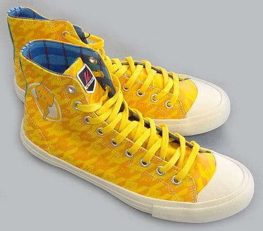
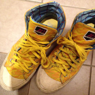
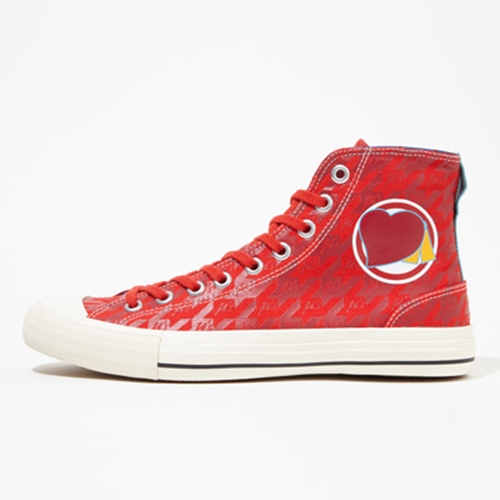
ラブライブ!×UBIQ コラボシューズ RIN
(税込) 送料込み
商品の説明
ラブライブ!×UBIQとのコラボシューズ。
カラー YELLOW サイズ 27.0
箱付き、替えの靴紐付きです。箱のまま保管していましたので、若干の擦れと箱傷みあります。
箱付きのまま、段ボール梱包にて発送致します。
虹ヶ咲学園スクールアイドル同好会
大西亜玖璃 上原 歩夢
相良茉優 中須 かすみ
前田佳織里 桜坂 しずく
久保田未夢 朝香 果林
村上奈津実 宮下 愛
鬼頭明里 近江 彼方
楠木ともり 優木 せつ菜
指出毬亜 エマ ヴェルデ
田中ちえ美 天王寺 璃奈
小泉萌香 三船 栞子
内田秀 ミア テイラー
法元明菜 鐘 嵐珠 ショウ ランジュ
矢野妃菜喜 高咲 侑
ラブライブ
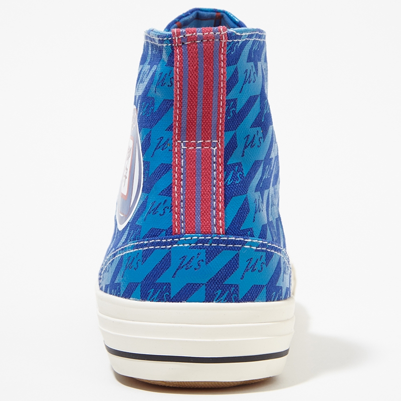
μ"s
高坂 穂乃果 新田恵海
南 ことり 内田彩
園田 海未 三森すずこ
小泉 花陽 久保ユリカ
西木野 真姫 Pile
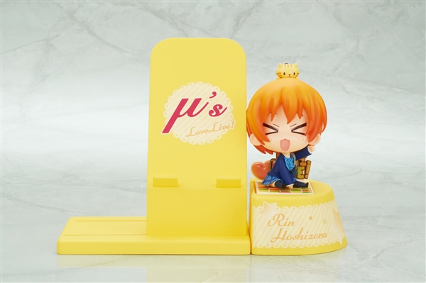
星空 凛 飯田里穂
東條 希 楠田亜衣奈
絢瀬 絵里 南條愛乃
矢澤 にこ 徳井青空
ラブライブサンシャイン
Aqours
高海 千歌 伊波杏樹
渡辺 曜 斉藤朱夏
桜内 梨子 逢田梨香子
黒澤 ルビィ 降幡愛
国木田 花丸 高槻かなこ
津島 善子 小林愛香
松浦 果南 諏訪ななか
黒澤 ダイヤ 小宮有紗
小原 鞠莉 鈴木愛奈
ラブライブスーパースター
Liella!
澁谷 かのん 伊達さゆり
唐 可可 Liyuu
嵐 千砂都 岬なこ
平安名 すみれ ペイトン尚未
葉月 恋 青山なぎさ
コースター
ブロマイド
フェス
ポストカード
キャラクター···コミック・アニメ・ゲーム
グッズ種類···プライズ/一番くじ商品の情報
| カテゴリー | おもちゃ・ホビー・グッズ > その他 > その他 |
|---|---|
| 商品の色を | オレンジ系 / イエロー系 / ホワイト系 |
| 商品の状態 | 目立った傷や汚れなし |
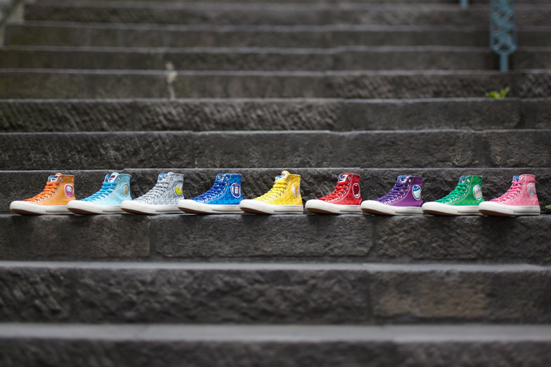
![ラブライブ!] ラブライブ!× UBIQ オリジナルスニーカー発売の](http://news.lovelive-anime.jp/app-def/S-102/news/wp-content/uploads/2015/06/all.jpg)
ラブライブ!] ラブライブ!× UBIQ オリジナルスニーカー発売の
駿河屋 -<中古>星空凛 スニーカー イエロー 29cm 「ラブライブ!×UBIQ
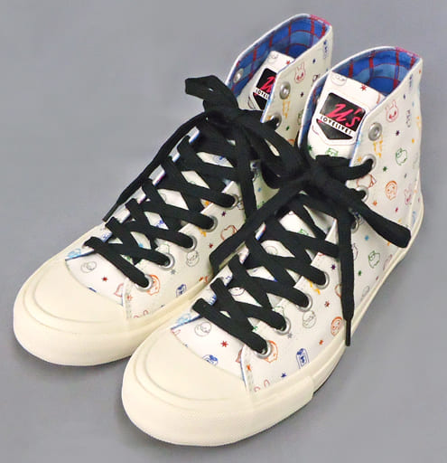
駿河屋 -<中古>μ's スニーカー ホワイト 27cm 「ラブライブ!×UBIQ RIN
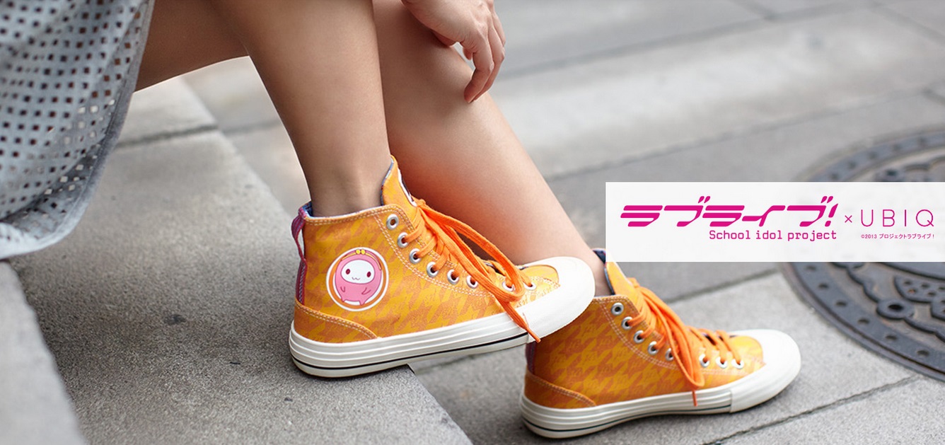
μ'sメンバーが足元をカラフルに彩る、【ラブライブ!】と【UBIQ】の

2023年最新】ラブライブ UBIQの人気アイテム - メルカリ
足元から青春がきこえる 「ラブライブ!」と「UBIQ」のコラボ

駿河屋 -<中古>μ's スニーカー ホワイト 26cm 「ラブライブ!×UBIQ RIN

駿河屋 -<中古>μ's スニーカー ホワイト 26cm 「ラブライブ!×UBIQ RIN
UBIQ - ラブライブ×UBIQの通販 by ガチオタ堂|ユービックならラクマ
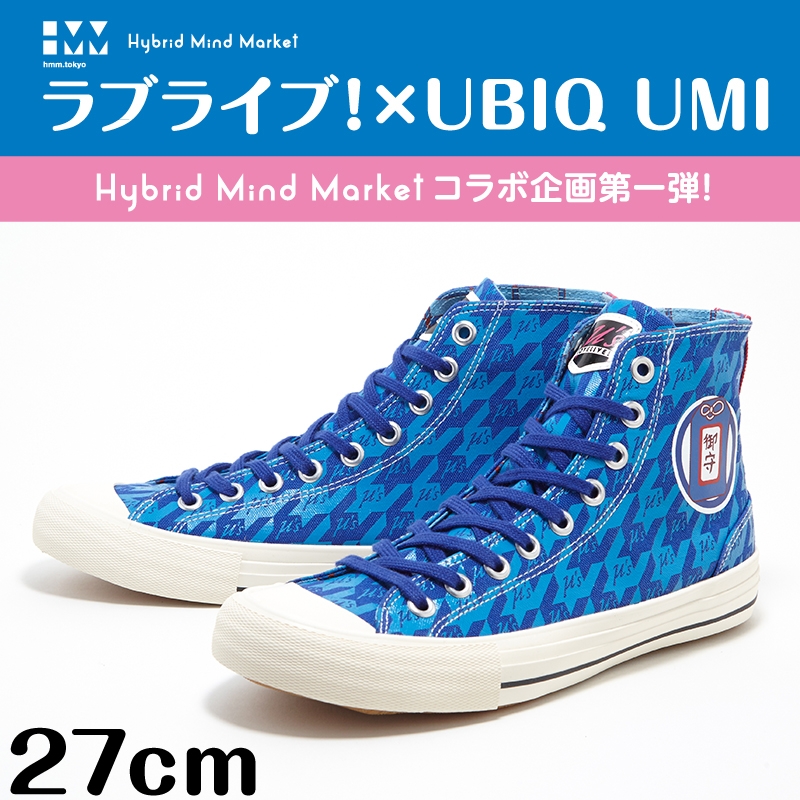
園田海未スニーカー【27cm】/ ラブライブ!×UBIQ UMI | HMV&BOOKS
![ラブライブ!] ラブライブ!× UBIQ オリジナルスニーカー発売の](http://news.lovelive-anime.jp/app-def/S-102/news/wp-content/uploads/2015/06/2.jpg)
ラブライブ!] ラブライブ!× UBIQ オリジナルスニーカー発売の

駿河屋 - 【買取】μ's マルチスニーカー ブラック 23cm 「ラブライブ
UBIQ - ラブライブ×UBIQの通販 by ガチオタ堂|ユービックならラクマ

ラブライブ!×UBIQ RIN スニーカー 星空凛 (25cm) ラブライブユービックスニーカー
![ラブライブ!] ラブライブ!× UBIQ オリジナルスニーカー発売の](http://news.lovelive-anime.jp/app-def/S-102/news/wp-content/uploads/2015/06/3.jpg)
ラブライブ!] ラブライブ!× UBIQ オリジナルスニーカー発売の
μ'sメンバーが足元をカラフルに彩る、【ラブライブ!】と【UBIQ】の
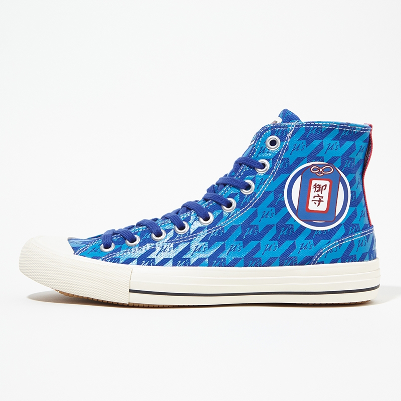
園田海未スニーカー【27cm】/ ラブライブ!×UBIQ UMI | HMV&BOOKS
UBIQの靴 - 通販 - hanackenovinky.cz
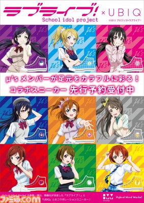
μ'sメンバーが足元をカラフルに彩る! “ラブライブ!× UBIQ
![ラブライブ!] ラブライブ!× UBIQ オリジナルスニーカー発売の](http://news.lovelive-anime.jp/app-def/S-102/news/wp-content/uploads/2015/06/poster.jpg)
ラブライブ!] ラブライブ!× UBIQ オリジナルスニーカー発売の

Aqours×R4Gコラボ ハイカットスニーカー ラブライブ!サンシャイン

駿河屋 - 【買取】園田海未 スニーカー ブルー 23cm 「ラブライブ

UBIQの靴 - 通販 - hanackenovinky.cz
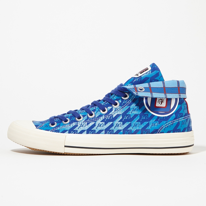
園田海未スニーカー【27cm】/ ラブライブ!×UBIQ UMI | HMV&BOOKS

Aqours×R4Gコラボ ハイカットスニーカー ラブライブ!サンシャイン

未使用 ラブライブ× UBIQ 凜ちゃんコラボ スニーカー サイズ27cm
ラブライブ!Official Web Site | ニュース

楽天市場】UBIQ×ラブライブ! INSOLE(ユービック×ラブライブ

UBIQの靴 - 通販 - hanackenovinky.cz

2023年最新】ラブライブ UBIQの人気アイテム - メルカリ
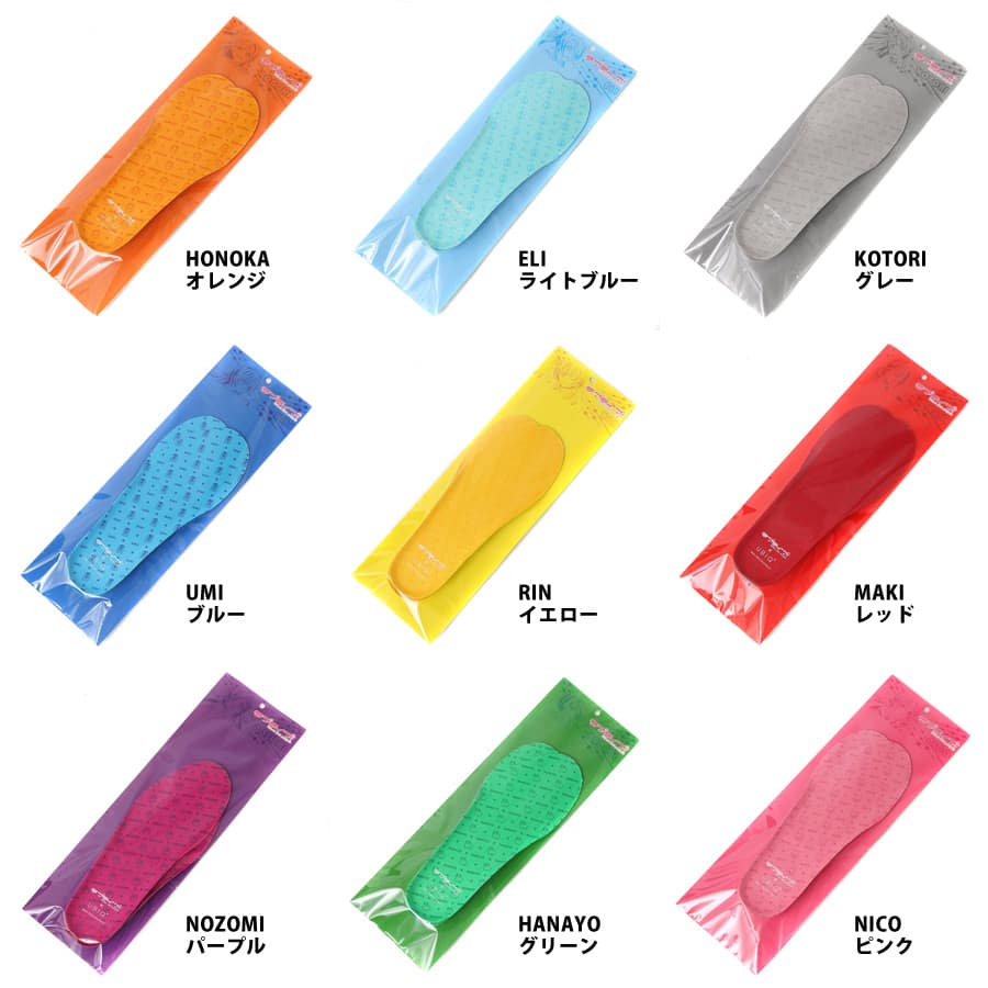
UBIQ×ラブライブ! INSOLE 9色展開 15FW-S
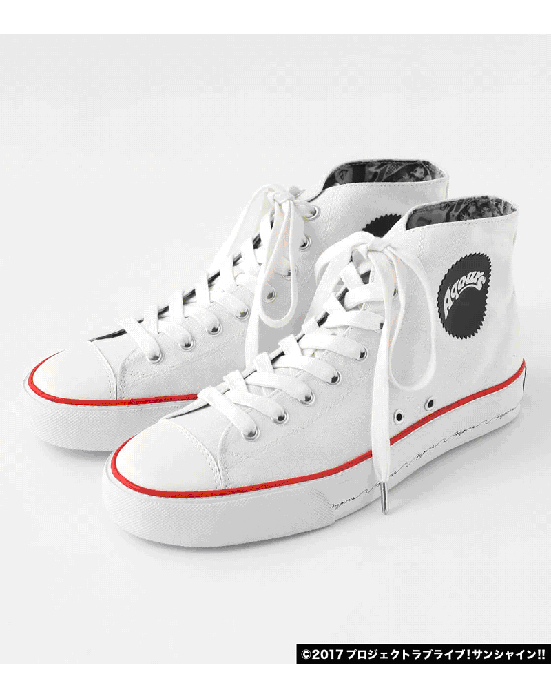
ラブライブ!サンシャイン!!』待望のスニーカーの発売が決定! | R4G
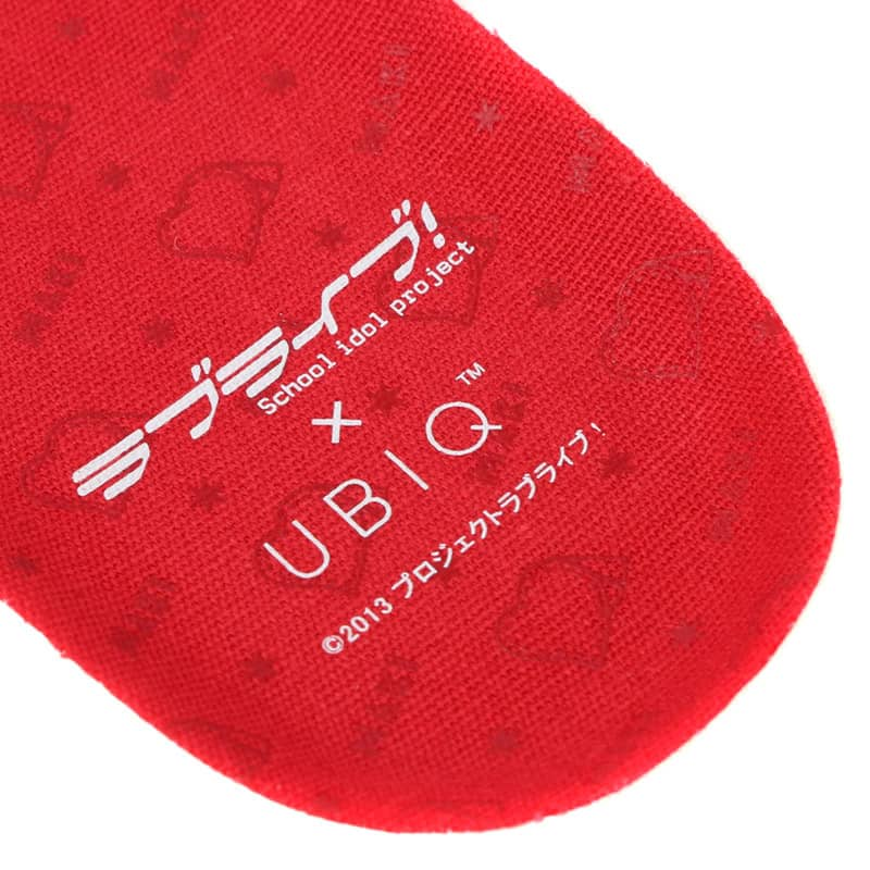
UBIQ×ラブライブ! INSOLE 9色展開 15FW-S

UBIQの靴 - 通販 - hanackenovinky.cz
園田海未スニーカー【27cm】/ ラブライブ!×UBIQ UMI | HMV&BOOKS
ラブライブ!Official Web Site | ニュース
μ'sメンバーが足元をカラフルに彩る、【ラブライブ!】と【UBIQ】の

ラブライブ スニーカーのヤフオク!の相場・価格を見る|ヤフオク!の

駿河屋 - 【買取】高坂穂乃果 スニーカー オレンジ 25cm 「ラブライブ
ラブライブ!× ユービックとのコラボオリジナルスニーカーが予約受付中


商品の情報
メルカリ安心への取り組み
お金は事務局に支払われ、評価後に振り込まれます
出品者
スピード発送
この出品者は平均24時間以内に発送しています


